PCB Design Services
Inner Systems take up all kinds of Analog, Digital, RF or mixed signals PCB design services. We have capabilities of designing high speed, impedance controlled multi layer PCBs up to 32 layers. We have expertise in the field of Telecommunication, Automation, Defence, Automobiles, Security, Medical, Power supply and education etc. During design process we adopt several design rules, like routing topology, length matching, differential pairs, EMI/EMC, impedance control etc. All these rules may not be applicable to all the PCBs but mostly used in high speed PCBs. For power supply, in high current path we provide appropriate copper trace width and thickness. When there is a mixed signal PCB, we follow the standard isolation method. RF boards are designed as per the impedance specified by the design engineer. All the care will be taken as per the customer specifications and documents provided.
The PCB design begins with import of net list, assigning board area and placement of components. Obviously placement of components as per the flow is a very essential point. Every section of components will be arranged such a way that, there should be no conflict in any form. We can able to manage all kinds of components in our design. There are various kinds of components with different packages and form factor available in the market. The present day’s components have shrunk in to such a small sizes with much closer pin pitch arrangements and become more complex in PCB design. We adopt all kinds of fine pitch components like, TQFP, LQFP, PQFP, QFN, DFN, LPCC, LFCSP, MSOP, PDSO, QSOP, SOP, SSOP, TSSOP, SOT, BGA, PGA, FBGA, VFBGA, LGA, PLCC, SOD, SOT etc. We have also applied SMD and Press fit Connectors in many of our past designs. For discrete components minimum 0201 footprint can be used.
We also design Rigid Flex and Flex PCBs. For compact systems this kind of designs are advantages to fit in tight spaces. Flex PCB can be designed from 1-6 layers but it is advisable to keep maximum of 2 layers for better cost effective and flexibility.

PCB DESIGN INPUTS REQUIRED
>> We accept schematic in any format, may be hand drawn, PDF file or Design file of relative EDA tools.
>> Mechanical drawing with dimension, mounting holes position and component placement constraint.
>> Preferably in DXF format, if not available PDF format is acceptable.
>> Data sheets of electronic and mechanical components in PDF format
to create footprint and mechanical components..
>> Based on the mechanical inputs we will prepare Board outline for component placement..
>> In case of high speed board we need a list of critical signals and the preferred layer stack up.
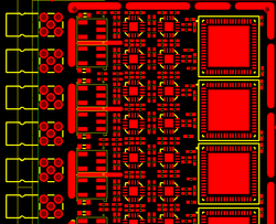
>> Shown is a sample schematic and placement of the board.
PCB TECHNOLOGY APPLICABLE
>> Single, Double side and multi layer board.
>> High speed Multiplayer board up to 32 layers
>> Single ended with 50 ohm and Differential pair with 100 ohm, 90 ohm, 85 ohm and 120 ohm impedance routing.
>> Fine pitch Footprint creation as per IPC standard minimum of 0.4 mm pitch.
>> High speed design Rules with EMI/EMC,Impedance controlled routing,
>> Length matching, Differential pairs routing,
>> Split Power Plane and Ground Plane etc.
>> Power driven traces with current ratings.
>> Rules driven Design.
 |  |  |
|---|
ADOPTED PCB DESIGN FLOW
* Schematic Capture
* Footprint Creation
* Footprint Allocation
* Net list generation
* Import net list to layout Tool.
* Set Board outline as per given inputs
* Placement of critical components as per drawing instruction.
* Placement of all components as per group and flow
* Set up design rules
*High speed signal constraint management and set up.
* Fan out of Power and Ground nets.
* Routing step by step on priority basis.
* DRC verification and Cleanup process.
* Arrange legends and Logos.
* Generating Gerber RS274X, Drill Data, Assembly and other,
* output files for PCB Manufacturing and Assembly.
* Verification of Gerber files with CAM tool.
DELIVERABLES
* Schematics drawing.
* BOM in Excel format.
* Gerber Files for PCB fabrication.
* Fabrication Drawing.
* Assembly Drawing.
* Pick and Place data.
* Paste mask file for Assembly.
* DXF file for Mechanical assembly.
* 3D files for Mechanical assembly.